In-Situ TEM
In situ Heading link
Energy storage has been identified as a major bottleneck in transportation, energy production, and electronic device technologies. In particular, all of these utilize rechargable batteries, where an ion such as Li or Mg travels from the anode end to the cathode end during discharge. Design of appropriate hosts for the Li, Mg, or other ions necessitates observing the atomic-scale processes involved in intercalating the ion into the material. Intercalation of the ion both reversibly and irreversibly alters the host. Understanding these processes is fundamental to the design of new high-capacity, high-rate batteries for the next generation of technology. Aberration-corrected scanning transmission electron microscopy (STEM) provides atomic resolution imaging, coupled with chemically sensitive electron energy-loss (EELS) and energy dispersive x-ray (EDS) spectroscopies, and lends direct insight into the physical mechanisms controlling charging and discharging processes.
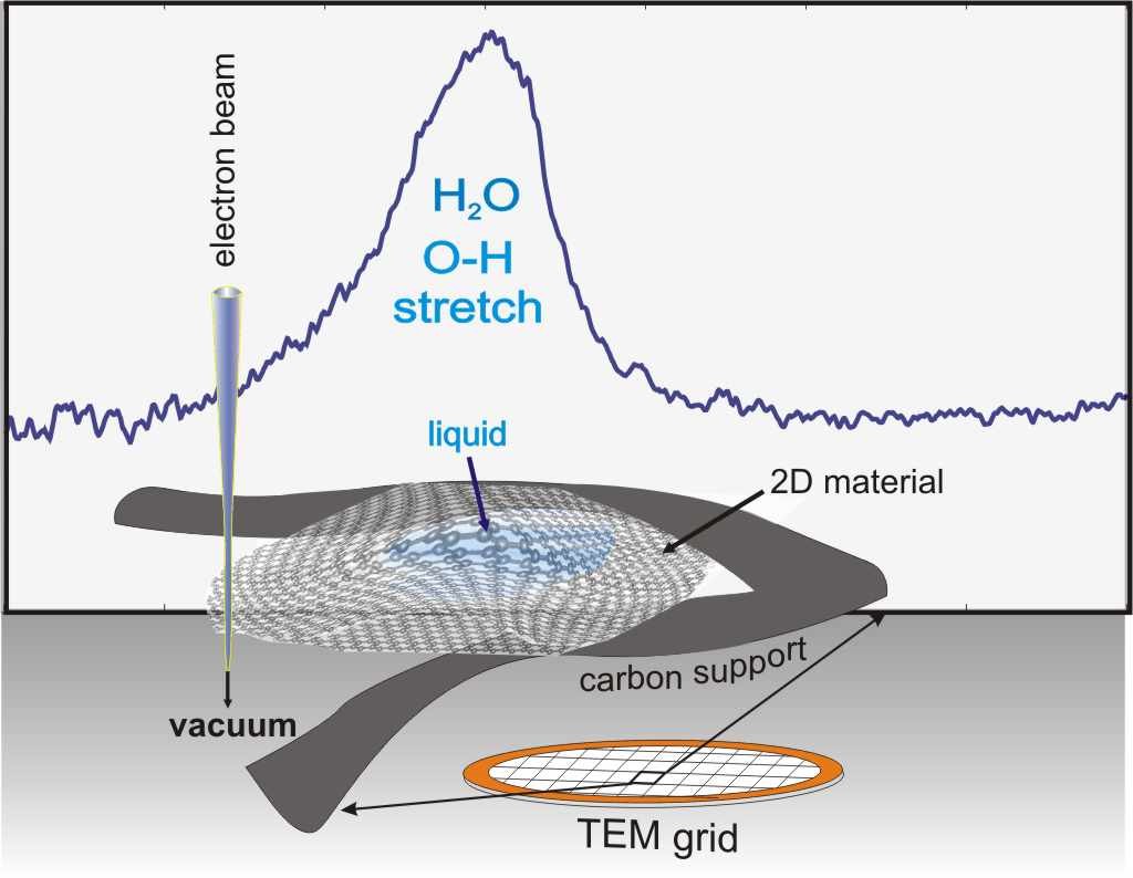
Meanwhile, liquids and liquid interfaces play a significant role in many, many processes, yet understanding nanoscale interactions in liquid environments has proved exceptionally difficult. Recent advances in electron microscopy have allowed the construction of silicon chip-based encapsulated liquid environments allowing imaging and in situ probing at resolutions approaching single-nanometer. However, to make full use of the atomic-scale spatial resolution, as well as EELS and EDS analysis, thinner window materials encapsulating smaller liquid droplets are required. Utilizing graphene or other 2D materials , 35-50 nm thick liquid cell samples containing a large variety of samples from organics to nanoparticles can be realized, and the interaction between liquid and sample probed at resolutions approaching the atomic scale. Leveraging the most modern monochromated electron sources, it is even possible to conduct vibrational spectroscopy at better than 10 nm spatial resolution. A schematic example is shown in the figure. This new window to the nanoscale has immense potential for a wide range of scientific disciplines.
References:
- “Vibrational spectroscopy of water with high spatial resolution,” J.R. Jokisaari, J.A. Hachtel, X. Hu, A. Mukherjee, C. Wang, A. Konecna, T.C. Lovejoy, N. Dellby, J. Aizpurua, O.L. Krivanek, J.C. Idrobo and R.F. Klie, Advanced Materials (in print)
- “Bio-camouflage of anatase nanoparticles explored by in situ high-resolution electron microscopy,” A.R. Ribeiro, A. Mukherjee, X. Hu, S. Shafien, R. Ghodsi, K. He, S. Gemini-Piperni, C. Wang, F. Klie, T. Shokuhfar, R. Shahbazian-Yassar, R. Borojevic, L.A. Rocha, J.M. Granjeiro, Nanoscale, 9 (30), 10684-10693 (2017)
- “Precise In Situ Modulation of Local Liquid Chemistry via Electron Irradiation in Nanoreactors Based on Graphene Liquid Cells,” C. Wang, T. Shokuhfar and F .Klie, Advanced Materials, 28(35), 7716 (2016)
- “High-Resolution Electron Microscopy and Spectroscopy of Ferritin in Biocompatible Graphene Liquid Cells and Graphene Sandwiches,” Wang, Q. Qiao, T. Shokuhfar, and R.F. Klie, Advanced Materials, 26, 3410-3414 (2014)